FIB - Crossbeam Cryo-FIB

Zeiss Crossbeam 550 Cryo-FIB

The Zeiss 550 Crossbeam FIB-SEM is a highly versatile instrument that combines high-resolution SEM imaging with advanced FIB capabilities, enabling TEM lamella preparation, nanofabrication, and 3D analysis for materials and life sciences. The 550 Crossbean consists of a Gemini 2 SEM and the new Ion-sculptor Ga-FIB column, with platinum and carbon gas injection systems for in-situ deposition. A Kleindiek manipulator supports both RT and cryogen lamella lift-out solutions.


For further information, contact Charlie Kong and Juanfang Ruan.

Life Sciences

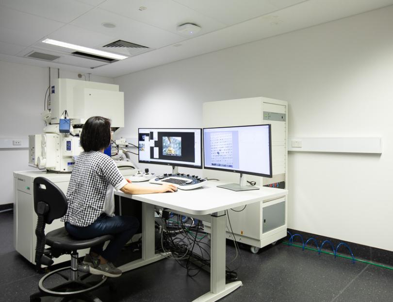
The Crossbeam 550 is equipped with a Quorum cryo-stage and cryo-transfer system, which facilitates serial block face imaging and TEM lamella preparation from cells or tissues for high-resolution cryo-TEM imaging at cryogenic temperatures. The instrument also supports cryo-SEM imaging, TEM lamella preparation and 3D volume imaging for plastic-embedded tissue blocks.

The Crossbeam 550 can be used with our correlative cryogenic workflow, consisting of a Linkam Scientific cryo-stage (CMS196), confocal LM (ZEISS LSM900 with Airyscan) and ZEN Connect software. This enables a seamless correlative cryo workflow that connects various microscopy techniques between cryo light microscopy, cryo-FIB and cryo-TEM.

Materials Science

This Ga-based FIB is a powerful platform for site-specific 2D and 3D analytical applications. Combining SmartFIB with advanced drift correction enables sophisticated stage motion control for automatic milling and serial data collection from multiple regions of interest. This provides a user-friendly workflow for nanofabrication, cross-sectional milling and imaging, and fabrication of ultrathin lamellae for further TEM analysis. The Crossbeam 550 is also equipped with an Oxford Ultim Max 170 SDD EDS system, which enables simultaneous data collection with high-resolution elemental analysis and imaging capabilities. The Atlas 5 software package provides an advanced design programming environment for nanofabrication and 3D EDS volume imaging.