2018 images of the month

September 2018

Yu Zhang (YoYo)School of Photovoltaic and Renewable Energy Engineering (SPREE)

Platinum deposited on a silicon wafer

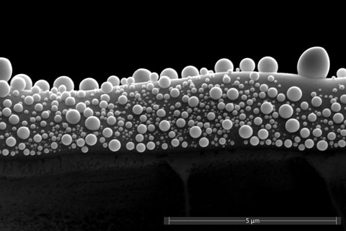
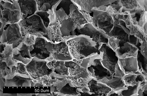
This SEM image shows the cross-section of a silicon solar cell TEM sample prepared the using in-situ liftout technique. Top side is a 3um thick Pt later deposited on top of silicon wafer in order to protect the surface morphology, bottom side is the silicon substrate. When transferring the micro-sized sample from its original place into sample grids, people need to weld sample by Pt deposition. The deposition current is too high so excessive local heat recrystallize the Si sample and re-shape the top Pt layer into micro/nano-spherical structure.

Image by: Yu Zhang

Supervisors: A/Prof. Bram Hoex & Dr.David Payne

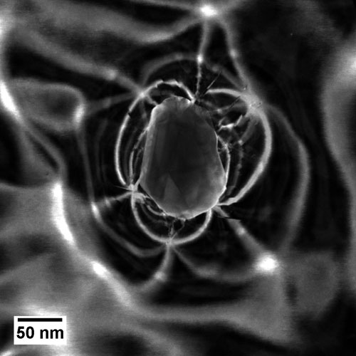
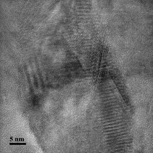
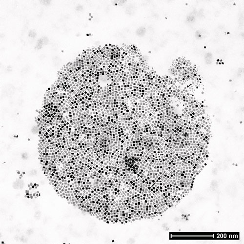
Microscope/Technique: PFIB, TEM sample Insitu Liftout

June 2018

Nor Akma Ismail - School of Chemical Engineering

Rice bran surface

This image shows the surface structure of rice bran that has been treated with Ultrasound at maximum amplitude. The rice bran surface structure has become very porous.  Distribution of resistant starch particle has also observed in the porous structure.

Image by: Nor Akma Ismail

Supervisor: A/Prof Jian Zhao

Microscope/Technique: Hitachi s3400

May 2018

Xianjue Chen - School of Chemistry

Gold particle on gold nano-sheet

This image shows a gold particle (~50 nm in size) sitting on top of a piece of ultrathin gold nano-sheet of ~5 nm in thickness. The weight of the particle causes local bending of the sheet, which induces a “spider web” like pattern under scanning transmission electron microscopic imaging.

Image by: Xianjue Chen

Supervisor: Prof. Chuan Zhao

Microscope/Technique: JEOL f200, STEM

March 2018

Paria Sadat Musavi Gharavi - School of Material Science

High resolution image of interface between GaP and ZnS

This image shows the interface between GaP and ZnS, which were grown as a multilayer film on silicon.  The interface between GaP and ZnS hosts infinitive three-dimensional (3D) defects such a plan of vacancies and dislocations or a plan of twinning. A considerable enhancement of photoactivity is found at multilayered structure containing plenty of twin boundaries compared with twin-less samples using a new definition of “Twin boundary engineering”.

Image by: Paria Sadat Musavi Gharavi

Supervisor: Prof. Nagarajan Valanoor

Microscope/Technique: JEOL f200 TEM 

January 2018

Hsiang-Sheng (Johnson) Cheng - School of Chemistry

Pt3Sn nanoparticles

The image shows uniformly-sized ordered Pt3Sn cubes and right bipyramids mainly bounded by (100) facets. The pyramids provided the flexibility of the way particle assemble, breaking the stern 90 degrees given by the sub-10 nm nanocubes forming all kinds of curved pattern. 

Image by: Hsiang-Sheng (Johnson) Chen

Supervisor: Prof. Richard Tilley

Microscope/Technique: Tecnai