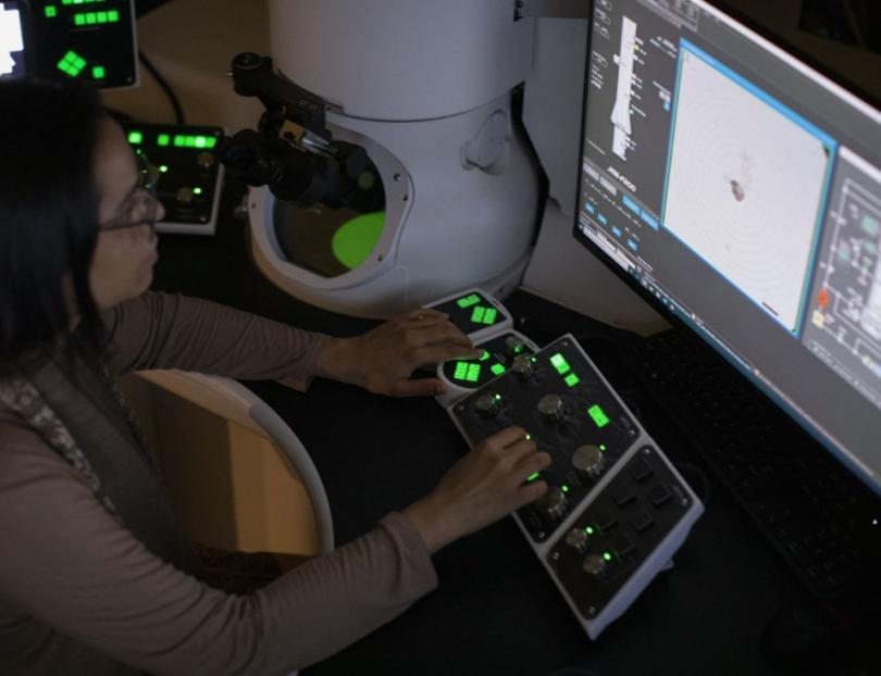
The JEOL F200 in F10 has been specially configured for high-resolution imaging and analytical tasks. It is well-suited for various materials samples, including nanoparticles, metals, semiconductors, photovoltaics, and ferroelectric materials. This microscope is ideal for fast elemental mapping at sub 1 nm resolutions.
The JEOL F200 is a versatile analytical transmission electron microscope (TEM) and scanning transmission electron microscope (STEM) that is well-suited for routine high-resolution work of materials samples. It can image nanoparticles, metals, semiconductors, photovoltaic materials, and ferroelectric materials with atomic resolution. F200 (E10) has a cold field emission gun (FEG) that can operate at 200 kV or 80 kV (under special request). The high brightness and coherence of the cold FEG mean that this microscope is ideally suited for analytical microscopy of materials. The F200 has a lattice resolution of 0.16 nm in ADF STEM mode and 0.1 nm in TEM mode at 200 kV.
The F200 is equipped with a JEOL 100 mm2 energy-dispersive X-ray (EDX) detector, with an energy resolution of 130 eV (Mn K) and a collection angle of 0.9 steradian. The F200 EDX efficiently collects X-rays from the sample, resulting in high-quality elemental maps.


